
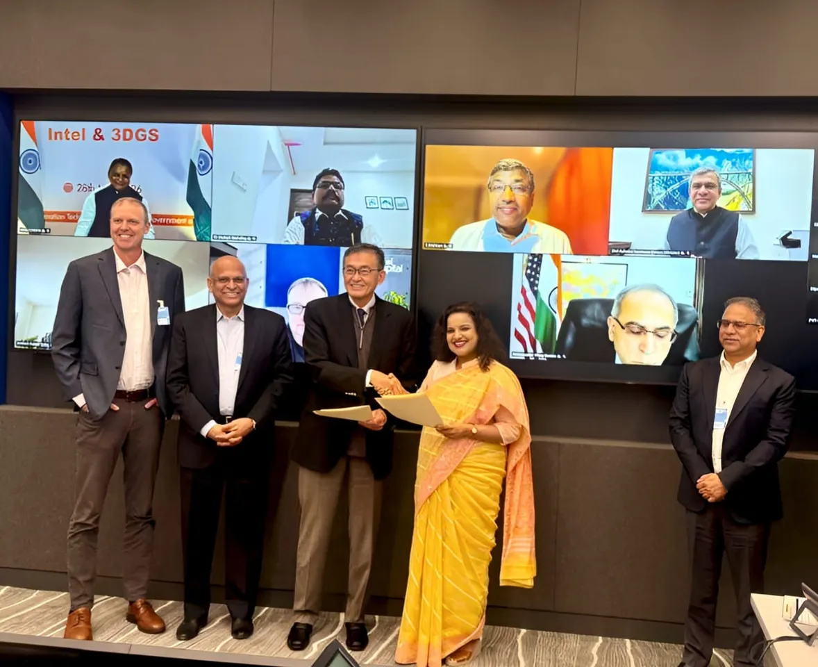
Odisha has taken a significant step towards becoming a major player in India’s semiconductor ecosystem with the signing of a landmark Memorandum of Understanding (MoU) between the Government of Odisha, Intel Corporation, and US-based 3DGS Inc. to establish an Advanced Packaging Glass Core Substrate Manufacturing Facility in the Bhubaneswar-Khordha region.
The agreement, witnessed by Union Electronics and Information Technology Minister Ashwini Vaishnaw, Odisha Chief Minister Mohan Charan Majhi, Intel CEO Lip-Bu Tan, and other senior dignitaries, marks one of the largest high-technology manufacturing investments proposed in the country’s semiconductor sector.
The upcoming facility will focus on the production of advanced packaging glass core substrates, high-density interconnect substrates, and other cutting-edge semiconductor technologies. Intel will contribute technology expertise and process know-how, helping strengthen India’s capabilities in semiconductor manufacturing, advanced packaging, and global supply chain integration.
Highlighting the significance of the project, Union Minister Ashwini Vaishnaw said the partnership reflects growing global confidence in India’s semiconductor ambitions under the India Semiconductor Mission. He noted that the involvement of leading global technology companies demonstrates the country’s emergence as a preferred destination for high-end electronics manufacturing and innovation.
Vaishnaw pointed out that collaborations involving global industry leaders such as Applied Materials, Lam Research, Tokyo Electron, Merck Electronics, ASML, and Tata Electronics are helping build a robust semiconductor ecosystem in India. According to him, the Odisha project will further strengthen domestic manufacturing capabilities and support the country’s vision of technological self-reliance.
The project is expected to be implemented in phases over the next five to six years. Besides creating a large number of high-skilled direct jobs, it is also expected to generate substantial indirect employment opportunities across the manufacturing, engineering, logistics, and technology sectors.
Chief Minister Mohan Charan Majhi described the agreement as a transformative opportunity for Odisha. He said the project would not only attract investment but also promote innovation, skill development, and industrial growth while positioning the state as a key destination for advanced technology manufacturing.
The facility is expected to play a crucial role in developing India’s advanced semiconductor packaging capabilities, an area that has become increasingly important in the global electronics industry. Experts believe the project could help reduce dependence on imports, strengthen domestic supply chains, and enhance India’s competitiveness in the international semiconductor market.
The initiative aligns with the broader objectives of the India Semiconductor Mission, which aims to establish a comprehensive semiconductor and electronics manufacturing ecosystem, attract global investments, and create world-class technology infrastructure across the country.
With the proposed facility in Odisha, India moves closer to its goal of becoming a global hub for semiconductor manufacturing, advanced packaging technologies, and next-generation electronics production.